an applet-based variable size-scale adventure for
nano-microscopy explorers
Below find an interactive model
representing a transmission
electron microscope specimen similar in size to the
grid shown on the right,
next to an ordinary staple. The model is of a
rigid self-supporting specimen like that sometimes
used for the study of semiconductors and layered
metal/ceramic devices, nominally prepared by cutting
a 3-mm diameter disc, thinning via abrasion to 100 micron thickness,
dimpling from one side with a specialized
milling machine, and then perforation by argon
ion milling. Using your mouse, you can rotate, spin,
as well as zoom around on or even inside the
structure, thanks to an intersecting-axis goniometer
with no rotation limits.
The 31 sections of the specimen nearest the
perforation in the center taper down to zero thickness.
These are the regions which are most
interesting for transmission electron microscopy.
However the wide tilts, the large focal depth, and the
geometric contrast mechanisms of the web-microscope used
here allow one to also obtain topographic information of
the sort that atomic force and scanning electron microscopes
can generate. We have plans to allow you to explore
this and other specimens on the micron, nanometer, and even
atomic scales in the days ahead, as well as
to taylor stories for the use of such models
in classrooms from kindergarten through grad school.
One objective is to provide visitors with a visceral
feel for scale changes that the nano-explorer
experiences, in the process of "getting small".
How astute are your
observational skills? What information would you bring
back from a "fantastic voyage" into the nanoworld? Don't mind the
curious duck in the background, as long as it keeps some
distance. If you look carefully, you may
already be able to find a bit of pollen, a few red blood cells, a couple of
tobacco mosaic virus particles, a carbon nanotube, and
even a buckyball with a few metal atoms hanging around.
Of course, unfamiliar contrast mechanisms are needed to observe objects
smaller than the wavelength of light, so be prepared for a few
surprises.
Note: The mouse allows you to
re-orient and or spin the specimen, while the Shift key plus
vertical mouse motion allows zooming in on the model for a closer look.
The Home key returns you to the original
point of view, and the buttons above let you estimate goniometer
angles and field-width. The rotation-center may be moved
along scope cartesian (xyz) axes by tapping the xXyYzZ
keys (hint: rotate between taps). If this version bogs down on zooming (e.g. with an older PC),
try a 400x400
or 200x200
window. Try
this model
for less surface topography, and
this model
if you wish to rotate "the camera" rather than the specimen.
Puzzler #1: If the diameter of the disk is 3mm, what is
it's thickness at the outer edge? What is the
diameter of the perforation?
Puzzler #2: This is tougher: Estimate the
radius of the spherical dimple on one side of
the disk, as well as the distance the dimpling
wheel protruded through the perforation at the
end of the dimpling process. Note: One usually
stops dimpling before perforation, and perforates
by a gentler method e.g. argon ion milling, but
assume here (to be specific about geometry)
that the perforation was created by the spherical
dimple itself.
Puzzler #3: Perhaps equally tough, but
of more direct relevance to the microscopist:
Estimate the wedge-angle between intersecting
specimen surfaces at the perforation, and the
length of perimeter associated with each of the
31 sections which border the perforation.
Puzzler #4: Another practical
question for the microscopist: How
many square microns of specimen, whose thickness
is less than 0.5 microns, will the
microscopist find? If the objects of interest
occur 10^6 times per square centimeter of specimen,
how many objects are you therefore likely to find in
such thin areas of this specimen?
Puzzler #5: If the defects are
"bulk defects" much less than a micron in size,
the amount of "volume" of your specimen which
is thin becomes the important parameter.
How much volume of this specimen (in
cubic microns) is associated with parts
of this specimen which are less than 0.5
microns in thickness? If there are 10^10
of the interesting objects per cubic
centimeter, how many would you expect to
find in a survey of all such thin area
in this specimen.
Puzzler #6: What is the spacing
between squares of the smaller "secondary grid" that
you'll find somewhere near the edge of the perforation?
Hint: The distance is larger than the
wavelength of visible light, and perhaps 6 times
the feature width used in modern gigascale integrated
circuits.
Puzzler #7: As you zoom in, you may notice
a hierarchy of three more even smaller (e.g. call them
third, fourth, and fifth-level) grids at the
perforation's edge. These third, fourth, and fifth
level grids are not typically resolvable by light
microscopes, and hence constitute the primary domains
of electron and scanning probe microscopy. Most
scanning electron microscopes today can pick up
periodicities as small as those in the fourth-level
grid. Scanning tunneling and atomic force microscopes
(which mechanically scan a tip over the specimen)
under suitable conditions can pick up details smaller
than the fifth-level grid, as can conventional
transmission electron microscopes. How many such
fifth-level grid squares would be needed to outline
the whole perimeter of the perforation?
Note: Since mechanical
(scanning probe) microscopes use tips which are made
of atoms, sub-atomic lateral resolution is
difficult even though they can easily do sub-atomic
height profiling, but for decades transmission electron
microscopes have fallen into two categories:
the handful of atomic resolution scopes that can barely resolve
details smaller than the 2 Angstroms separation between
most atoms, and conventional scopes that cannot. This
is about to change with new aberration-correction
techniques, which will eventually allow us to see atomic
nuclei as little "points of light" in images.
Puzzler #8: Note that the "shoreline"
around the perforation is irregular. Can you
tell us anything about the frequency spectrum of
deviations from circularity, either with a seat
of the pants estimate, or via quantitative
analysis? Does the character of these
deviations change as one goes to smaller and
smaller sizes, or does the edge profile in
this specimen show signs of self-similarity?
Puzzler #9: Note that the dimpled
side of the specimen shows more roughness than
the non-dimpled side. Is the surface topography
self-similar on some or all size scales? On what
size scales does the roughness appear to associated
with bumps, scratches, pits, random 1/f topography, or
something else? If you see bumps, what distribution
of widths and heights do they have, and how many per
square centimeter do your observations suggest are
present? Likewise for pits or scratches. Do
possible causes for these features come to mind?
Can you put limits on the amount of root-mean-square
roughness per decade
of lateral frequency, on either side, between
one cycle per millimeter and one cycle per micron?
How about between one cycle per micron and
one cycle per nanometer?
Puzzler #10: Make note of the sizes
and shapes of the objects you find. For example,
what are the dimensions of
the pollen particle, the red blood cells, the
tobacco mosaic virus particles, the nanotube,
and the buckyball. Do the two tobacco mosaic
virus rods have the expected cross-sectional
shape? How many walls does the multi-walled
nanotube show? Is the
single-walled part of that nanotube of the
armchair, zig-zag, or chiral variety? Is there
anything which is atypical about it?
How many pentagons can be found on the surface
of the buckyball?
Puzzler #11: What are the distances between metal atoms in
those nearby clusters? Are the atom colors coordinated
with possible atom, or different unit cell, types? What
features make the various cluster types preferable, for those
atoms which adopt them?
Capture an image of each of the metal atom arrays viewed
down a three-fold symmetric projection. How many
three-fold directions does each of these arrays have?
Five-fold? Four-fold? Can you name the polyhedron associated
with each of these nearest neighbor cluster types? How might
you describe the structure and crystallographic orientation of
atoms which make up the specimen disc itself, in the sections
where they are visible. Does this structure suggest
values for the atomic number of these atoms (and hence
the chemical composition of this part of the
specimen)? If these are typical interatom spacings,
how many atoms are contained in the specimen
as a whole? What is the largest
projected spacing between rows of atoms visible
in these disc atoms? What lattice direction allows
one to view two of these wide spacings at once?
How many such lattice directions are there? If the
term "dimer row" is familiar to you, can you tell
which direction the dimer rows are running on the
flat (non-dimpled) underside of this region of the disc?
Can you explain how changes in this direction are often
associated with surface steps, easily seen by scanning
probe microscopes, which are less than an inter-atom spacing
in height?
Puzzler #12: If the model had a moveable rotation
center randomly located, could you find your way back to the
buckyball on a second visit? How might you describe it's
location in terms of the superposed grid hierarchy? For example,
might one say it's located in perimeter cell 14.9.3.4.9, or
something similar, where perimeter-cell numbering starts
from that part of the perimeter nearest the pollen grain?
If the grid lines weren't drawn on the specimen, what landmarks and
facts about the grid hierarchy might you note so that (if need
be) you could redraw the gridlines yourself on images from
the next visit? Also, can you determine the number of buckyballs
in perimeter-cell 1.1.1.1.1, without moving the rotation center?
Future Puzzlers: Is there anything yet to notice
about interfaces, or about point, line and extended
lattice defects? How would you recognize an
extrinsic stacking fault in this model? How would you determine
a dislocation's Burger's vector? How would you measure
strain?
Storylines for Classroom Use: Suggestions invited.
This is one of several web-based "active mnemonics", designed:
(i) to offer complementary perspectives and resources for achieving
present day teaching goals among students with a wide range of learning
styles; (ii) to do this in the context of emergent topics in modern
day science (e.g. nanoscale exploration, information physics,
allpaths/action/aging and metric-based anyspeed dynamics), many of which
have only begun to work their way into textbooks and curriculum goals; and
(iii) to be reliably available for use by individual teachers in class
and by students out of class. Nanoworld exploration is especially
interesting in this regard since it can offer an open-ended challenge
to one's skills at empirical observation and reporting, allowing
students to "participate in scientific investigations based on
real-life questions that
progressively approximate good science". This is, for example, a
primary goal of the K-12 Show-Me Standards on scientific inquiry,
the basis for Missouri Assessment Program tests.
Most classroom challenges instead focus on factual knowledge and
skills at theoretical prediction, perhaps since robust empirical
challenges have been more difficult to set up.
The generic storyline for probing student skills and biases
for empirical observation might go something like this:
"Someone has just prepared a specimen for a
closer look in your web microscope. You see it spinning
in front of the robot's image when you move your mouse
over the picture containing it. By dragging your mouse
with a button down, you can rotate or even spin the
specimen. By dragging the mouse vertically with the shift
key pressed you can move in toward the rotation center for
a closer look. Check out the specimen, and report back on
what you are able to find out." This of course will not be
specific enough for most students, or in fact most teachers.
By that same token, with added specifics it might prove
useful for students at various levels in topic areas ranging
from materials microscopy to gestalt psychology. Revisiting
the same model, with a new assignment in a different class, would
also reinforce students' corollary awareness of the challenges faced
in doing detective work at the nanoscale.
Thermal physics and uncertainty: Fleas on fleas on fleas...
(e.g. in a general studies course on the physical principles
underlying "how
things work"):
"In this exercise at empirical discovery, you will be assessed on your
ability to describe what you found and did not find, as well as on the
quality of the data you managed to come back with. Basically, so far
in this course we've talked of baseballs and tables and other macroscopic
objects as just that: Individual objects. In fact, they are composed of
tiny building blocks. A key parameter in thermal physics (e.g. the
way temperature works) turns out to be uncertainty about the
microscopic state of those building blocks. Since detective work on
these nanoscales is increasingly important in fields ranging from
engineering to medicine, this exercise gives you a feel for detective
work on the state of atoms making up a small 3mm disk." Assignment:
"Zoom in and around on the tiny disk that you'll find in this
web microscope. Feel free to assume the disk diameter is 3mm,
and to use the superposed grid to help estimate sizes of smaller
things. The field-width estimator can also be used, although this
might add additional uncertainty to your measurement. Then do the
best you can to determine the spacing between gray atoms in the
specimen's disk, a few of which are visible if you zoom in enough
to see them. In the panel below then report: (i) your measured value,
(ii) an estimate of your uncertainty in your measured value, and
(iii) a description of the method you used to come up with it."
Measuring Size Scales and Densities: Powers of 10... (e.g. as supplement
to the opening "measurement" chapter of a standard introductory physics
textbook): "Zoom down for a closer
look at this 3mm diameter web specimen, to see if you can determine
the distance between atoms in it, and/or the number of atoms it
contains per cubic centimeter." You might be inclined to let
them determine spacings on the superposed grids on their own.
Alternatively, you might tell them to assume that the level 2
grid squares are about a micron across, and the level 5 squares
about a nanometer across. Advantages to this exercise: It
is an experimental challenge (something students often don't
get outside of a lab), it offers a visceral feel for the
large number of intervening worlds between that of humans and
that of atoms, and it facilitates self-discovery about the nature
of these concepts in a cutting-edge but practical setting
frequented by today's nanoscale explorer.
Frequently Asked Questions: Suggestions invited.
How do I measure distances? You can assume that the diameter of
the disc is 3mm, and extrapolate all other dimensions from that. The
superposed grid lines may be of qualitative, and in some cases quantitative, help.
Serious detectives might also try to propagate uncertainties through the
extrapolation as well. On the other hand, your teacher may tell you to
start with different assumptions, e.g. the distance between atoms in a
certain object. The "Estimate Field Width" button may also come in
handy, although you might want to avoid taking the manufacturer's estimate
blindly at face value. Quantitative comparisons are probably best done between
objects whose distance from your vantage point is the same, and thus to set
up may require some rotation and zooming on your part.
How do I measure angles? In some cases the superposed
grid lines, or other aspects of the geometry of objects, can be
used to determine angles. Another trick for angles at the rotation
point might be to note that you can spin an object at a constant rate
of speed. If the spin takes you through the two directions of interest,
the angle between them is simply 360 degrees multiplied by the
time_between_directions divided by
the rotation_period. Given that the beta applet also allows you to
move the rotation center, in principle any two angles can be measured
with arbitrary precision (e.g. using slower rotations) by this means.
Lastly, the viewing direction is also roughly specified by values accessible
from the Tilt and Rotation angle buttons. For those who enjoy
spherical trigonometry, the angle between two
different viewing angles (e.g. T1,R1 and T2,R2) is
ArcCos[Cos[T1]Cos[T2]+Sin[T1]Sin[T2]Cos[R2-R1]].
How do I record observations for later analysis, and reports?
Although movies of what you see may be difficult to record, still photos
of what you see on the screen should be possible to print out using
File/Print (some browsers will let you select and print only the
applet window), or capture as digital images using
any of a number of screen capture utilities (e.g. Paint Shop Pro
under Windows) or even with a camera. When saving an image, it's
good practice to save relevant data (like field width at the rotation
center) along with it. For example, you might append "w6p67n" to
the filename of the image if the field width is 6.67 nanometers.
When recording images on film, microscopists generally record useful
information (along with the number of each negative) in a logbook.
This is also recommended here, since not all information corollary
to an image can be recorded in its filename. Note: Unlike
magnification, field width and scale bar labels are not changed
when the image is portrayed on larger or smaller screens. They also allow
one to easily determine magnification e.g. by dividing field width into
the width of the viewed image.
Future objectives
(for which technology is essentially in hand) include:
Push buttons to estimate the field width (now available),
goniometer angles, and working distance.
A couple of adenovirus particles and perhaps some other
stray molecules, hidden elsewhere on the specimen.
Ability to translate the rotation center in 3D, if
desired with a dynamically-regenerated grid overlay and specimen to
facilitate navigation plus offer non-trivial atom-scale detail
throughout the specimen. This may seem like a modest task until
one realizes that this specimen contains something akin to 10^20 atoms,
i.e. around 10^12 gigabytes of information encoded in atom
positions alone.
Ability to pass observation parameters back into a calculation engine that
can provide the explorer with HREM images, diffraction patterns,
X-ray or roughness spectra, etc. of
the field of view.
This page is
http://www.umsl.edu/~fraundor/nanowrld/dtemspec.html. Acknowledgement
is due particularly to
Martin Kraus
for his robust
Live3D
applet and
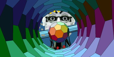
help adapting it to this application. A background image from
the Takanishi Lab
webpage on robot expressions has been put up
temporarily because we don't have a "first specimen" background
showing curious students looking at an object in the lab. Yet.
Although there are many
contributors, the person responsible for errors is P. Fraundorf. This
site is hosted by the Department of Physics and Astronomy (and Center for
Molecular Electronics) at UM-StL, and is part of the Physics Instructional
Resource Association webring (see below).
The number of visits here since last reset on 23 Aug 2003 is [broken counter].
Whole-site page requests est. around 2000/day hence more than 500,000/year.
Requests for a "stat-counter linked subset of pages" since 4/7/2005:


 and
help adapting it to this application. A background image from
the Takanishi Lab
webpage on robot expressions has been put up
temporarily because we don't have a "first specimen" background
showing curious students looking at an object in the lab. Yet.
Although there are many
contributors, the person responsible for errors is P. Fraundorf. This
site is hosted by the Department of Physics and Astronomy (and Center for
Molecular Electronics) at UM-StL, and is part of the Physics Instructional
Resource Association webring (see below).
The number of visits here since last reset on 23 Aug 2003 is [broken counter].
Whole-site page requests est. around 2000/day hence more than 500,000/year.
Requests for a "stat-counter linked subset of pages" since 4/7/2005:
and
help adapting it to this application. A background image from
the Takanishi Lab
webpage on robot expressions has been put up
temporarily because we don't have a "first specimen" background
showing curious students looking at an object in the lab. Yet.
Although there are many
contributors, the person responsible for errors is P. Fraundorf. This
site is hosted by the Department of Physics and Astronomy (and Center for
Molecular Electronics) at UM-StL, and is part of the Physics Instructional
Resource Association webring (see below).
The number of visits here since last reset on 23 Aug 2003 is [broken counter].
Whole-site page requests est. around 2000/day hence more than 500,000/year.
Requests for a "stat-counter linked subset of pages" since 4/7/2005: