[Background] [Live3D] [Puzzlers] [Storylines] [FAQ] [Links] [Downstream] [Acknowledgements]

Puzzler #1: If the diameter of the disk is 3mm, what is it's thickness at the outer edge? What is the diameter of the perforation?
Puzzler #2: This is tougher: Estimate the radius of the spherical dimple on one side of the disk, as well as the distance the dimpling wheel protruded through the perforation at the end of the dimpling process. Note: One usually stops dimpling before perforation, and perforates by a gentler method e.g. argon ion milling, but assume here (to be specific about geometry) that the perforation was created by the spherical dimple itself.
Puzzler #3: Perhaps equally tough, but of more direct relevance to the microscopist: Estimate the wedge-angle between intersecting specimen surfaces at the perforation, and the length of perimeter associated with each of the 32 sections which border the perforation.
Puzzler #4: Another practical question for the microscopist: How many square microns of specimen, whose thickness is less than 0.5 microns, will the microscopist find? If the objects of interest occur 10^6 times per square centimeter of specimen, how many objects are you therefore likely to find in such thin areas of this specimen?
Puzzler #5: If the defects are "bulk defects" much less than a micron in size, the amount of "volume" of your specimen which is thin becomes the important parameter. How much volume of this specimen (in cubic microns) is associated with parts of this specimen which are less than 0.5 microns in thickness? If there are 10^10 of the interesting objects per cubic centimeter, how many would you expect to find in a survey of all such thin area in this specimen.
Puzzler #6: What is the spacing between squares of the smaller "secondary grid" that you'll find somewhere near the edge of the perforation? Hint: The distance is larger than the wavelength of visible light, and perhaps 6 times the feature width used in modern gigascale integrated circuits.
Puzzler #7: As you zoom in, you may notice a hierarchy of three more even smaller (e.g. call them third, fourth, and fifth-level) grids at the perforation's edge. These third, fourth, and fifth level grids are not typically resolvable by light microscopes, and hence constitute the primary domains of electron and scanning probe microscopy. Most scanning electron microscopes today can pick up periodicities as small as those in the fourth-level grid. Scanning tunneling and atomic force microscopes (which mechanically scan a tip over the specimen) under suitable conditions can pick up details smaller than the fifth-level grid, as can conventional transmission electron microscopes. How many such fifth-level grid squares would be needed to outline the whole perimeter of the perforation? Note: Since mechanical (scanning probe) microscopes use tips which are made of atoms, sub-atomic lateral resolution is difficult even though they can easily do sub-atomic height profiling, but for decades transmission electron microscopes have fallen into two categories: the handful of atomic resolution scopes that can barely resolve details smaller than the 2 Angstroms separation between most atoms, and conventional scopes that cannot. This is about to change with new aberration-correction techniques, which will eventually allow us to see atomic nuclei as little "points of light" in images, and force us to add a sixth grid-level to illustrate their mapping capabilities.
Puzzler #8: Note that the "shoreline" around the perforation is irregular. Can you tell us anything about the frequency spectrum of deviations from circularity, either with a seat of the pants estimate, or via quantitative analysis? Does the character of these deviations change as one goes to smaller and smaller sizes, or does the edge profile in this specimen show signs of self-similarity?
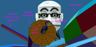
Puzzler #9: Make note of the sizes and shapes of the objects you find. For example, what are the dimensions of the pollen particle, the red blood cells, the tobacco mosaic virus particles, the nanotube, and the buckyball. Do the two tobacco mosaic virus rods have the expected cross-sectional shape? Is the single-walled part of the nanotube of the armchair, zig-zag, or chiral variety? How many pentagons can be found on the surface of the buckyball? What are the distances between metal atoms in those nearby arrays? Are the atom colors coordinated with possible atom types? What is the largest projected spacing between rows of atoms visible in the arrays? What lattice direction allows one to view two of these wide spacings at once? How many such lattice directions are there? Is there anything yet to notice about interfaces, or about point, line and extended lattice defects?
 .
A background image from
the Takanishi Lab
webpage on robot expressions has been put up
temporarily because we don't have a "first specimen" background
showing curious students looking at an object in the lab. Yet.
Although there are many
contributors, the person responsible for errors is P. Fraundorf. This
site is hosted by the Department of Physics and Astronomy (and Center for
Molecular Electronics) at UM-StL. The number of visits here since
last reset on 23 Aug 2003 is
.
A background image from
the Takanishi Lab
webpage on robot expressions has been put up
temporarily because we don't have a "first specimen" background
showing curious students looking at an object in the lab. Yet.
Although there are many
contributors, the person responsible for errors is P. Fraundorf. This
site is hosted by the Department of Physics and Astronomy (and Center for
Molecular Electronics) at UM-StL. The number of visits here since
last reset on 23 Aug 2003 is