Below find notes from a first attempt at quantitative analysis of one of our lattice images of Si/Si-Ge. Some of the data here is in the form of 4-panel image sets like those used in illustrations on our strain modeling page. It's only a first pass, but gives you an idea of how it might work. The Mathematica work-horse routines developed for this basically take a region of the strain map, and calculate average x and y components of the strain at each pixel, along with standard deviations and xy covariances. Error propagation is done using measured variances, plus standard error in the mean, and error propagation strategies (including covariance), ala Bevington.
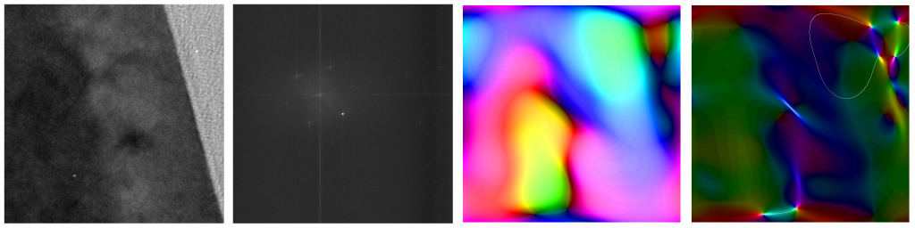
Before getting started, consider first some electron-optical (as distinct from digital-darkfield) diffraction contrast images of "local strain anomaly arrays" along the interface. Since the planar section specimens argue that these are not dislocations, it's gonna take some further thinking to figure out what they are. Strain relief would require misfits I think every 1.92*5.43/(5.477-5.43) or 220 Angstroms. The average space between the observed "crinkles" (below) in darkfield seems to be less than half that distance. Might they be providing some strain relief? If so, how? Might they, for example, be patches of partial coherence 5 to 10 nm across?
The above are "small aperture" or conventional TEM images. Below find closeup of a "large aperture" or high resolution (electron phase contrast) TEM image. The white dots have the periodicity of tunnels between silicon atom columns projected down the 110 silicon lattice direction. The calculations described below are done on such images, converting periodicity information into colors so that one can see interesting patterns which would otherwise be hidden. For example, one question we early on sought to answer was: Is that dark spot in this image (located near the Si/Si-Ge interface) associated with an edge-dislocation running toward us (out of the plane of the image)? The "extra plane termination" that one expects for edge-dislocations viewed end on is not seen if you inspect this image closely, and planar section work (like that described below) shows no sign of misfit dislocations at the Si/Si-Ge interface. Note: Quantitative analysis of strains in this image has only begun, and is not yet reported below.

Speaking of dislocations, here is what misfits microns deep in the Si-Ge transition layers look like in planar section (looking into the wafer surface)...

Caution below: The angle averaging routines might be having problems across branch cuts. More on that soon...
9am30mar2003: Although the sections immediately following, on negative 3049, illustrate the spirit of inquiry we've directed toward quantitative analysis of information in experimental megapixel digital-darkfield complex-color images, some foibles in Mathematica's handling of indices was at this time yielding numbers in the correct ballpark, but that did not represent precisely what we thought at the time. The numbers from negative 3051, further down, take into account the foibles referred to above. In addition they have subsequently been echoed in followup analyses of the negative 3049 crop discussed below. That means we're getting some quantititative agreement concerning (002) spacing variation normal to the strained Si interface, with images taken in two different locations along the interface.
1pm27mar2003: From the (002) strain analysis of a 1024x1024 crop of negative 3049, I calculated a strain (using a 306,299 pixel region on the Si-Ge side) with net phase 49 degrees (in the tensional direction, see below), and net amplitude of 0.0020+/-.0008. This means a change in phase of 0.002 [radians per pixel], or 0.002/2Pi [cycles per pixel]. 2Pi [radians] of course corresponds to a full period phase shift, for Si (200) of about 5.43/2=2.715 [Angstroms per cycle]. Also a 2400 [dpi] (or 2400/2.54 [dots per cm] or 100*2400/2.54 [dots per meter]) scan of a 240,000x image has 1/(240000*240,000/2.54) = 0.44 [Angstroms per pixel]. The change in lattice parameter associated with the strain is (5.43/2)(.002/2Pi)=0.000864 [Angstroms per pixel], each of which is 0.44 Angstroms wide. Dimensionless strain is therefore .000864/.44=0.00196+/-.0008. If the silicon has lattice parameter of 5.43[Angstroms] in the (002) direction, the effective lattice parameter of the Si-Ge in that direction must then be 1.00196*5.43=5.4407 Angstroms. For 20%Ge-Si we expect a bulk lattice parameter change to .2*5.66+.8*5.43=5.476 Angstroms. Thus we observe a lattice parameter increase in the Si-Ge of only about a quarter of that expected. Local variations in the (002) spacing near the interface might be even greater, if the interface is abrupt and coherent (e.g. between misfits) since the unit cells of the Si-Ge will be relatively squished along (220) near the interface and hence expanded even further in the (002) direction, the opposite effect i.e. (002) reduction operating in the Si above. If instead there is some diffusion of Ge into the strained Si, then one might expect a gradual rather than an abrupt and exaggerated transition. The main alternative to a misfit dislocation array (which planar section specimens show clearly is absent) is possibly a loss of (or only patchy) coherence. This might lessen the near-interface effects as well.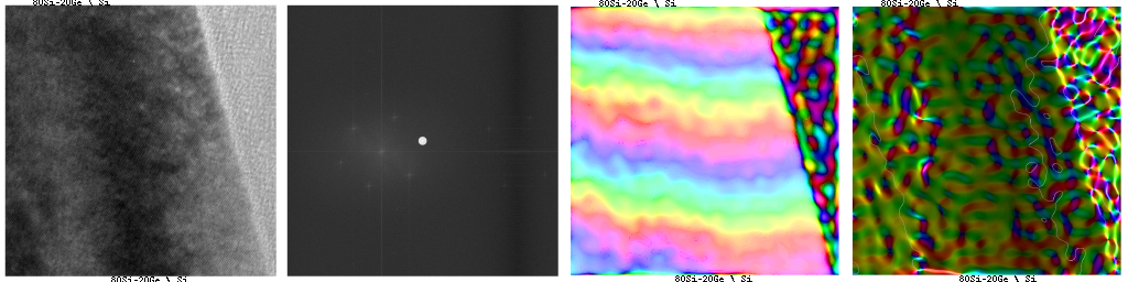
All of the foregoing is measured relative to the reference periodicity, which is near to that of the lattice on the Si-only (right) side of the image. On that side a similar calculation shows net strain down by about a factor of .002/.0005=4 (hence with a value in the noise). The blue (as distinct from yellow) spottiness in this region suggests that the reference periodicity is not totally noise, and may be between the Si-Ge and Si values. If we vector-subtract the net opposing strain directions (.002 at 49 degrees minus .0005 at -63 degrees), we get a vector strain relative to the top silicon lattice of .0022 at 61 degrees. This is about 45 degrees counter-clockwise from the (002) operating reflection and the wafer normal, meaning that the isotropic component of the strain is tensional. There is also a shear component in the direction of thinner silicon (upper left), although to the extent that the small Si-only strain is noise then it too may be noise. We haven't yet looked quantitatively at the thickness of the Si layer, at interface abruptness, or at specimen thickness dependences, since this is our first quantitative analysis of such an image. Next I'll try one of the two (111) reflections in this image. The signal to noise appears to be better there.
2:48pm27mar2003: Yes, the signal to noise is better. In our first (111) strain analysis on a 1024x1024 crop of negative 3049, I calculate from a 306,299 pixel region on the Si-Ge side a strain with net phase -172 degrees, and net amplitude of 0.0046+/-.0007. This means a change in phase of 0.0046 [radians per pixel], or 0.0046/2Pi [cycles per pixel]. 2Pi [radians] of course corresponds to a full period phase shift, for Si (200) of about 5.43/2=2.715 [Angstroms per cycle]. Also a 2400 [dpi] (or 2400/2.54 [dots per cm] or 100*2400/2.54 [dots per meter]) scan of a 240,000x image has 1/(240000*240,000/2.54) = 0.44 [Angstroms per pixel]. The change in lattice parameter associated with this is therefore (5.43/2)(.0046/2Pi)=0.00199 [Angstroms per pixel], each of which is 0.44 Angstroms wide. Dimensionless strain is therefore .00199/.44=0.00451+/-.0007. If the silicon has lattice parameter 5.43, the effective lattice parameter of the Si-Ge in that direction must then be 1.00451*5.43=5.454 Angstroms. For 20%Ge-Si we expect a bulk lattice parameter change to .2*5.66+.8*5.43=5.476 Angstroms. This might suggest a lattice parameter increase in the Si-Ge of about half of that expected.

All of this is measured relative to the reference periodicity, which however is quite near to that of the Si only (right) side of the image, where a similar calculation shows net strain of .00124+/-.0007, down by about a factor of .00459/.00124=3.7 but just out of the noise. The blue (as distinct from yellow) spottiness in this region (and net phase of -4.8 degrees) suggests that the reference periodicity is between the Si-Ge and Si values, so that that the calculation above is an underestimate of the lattice parameter difference relative to the strained silicon. If we vector subtract the opposing strain directions .0046 at -172 degrees minus .00124 at -4.9 degrees, we get a vector strain relative to the top silicon lattice of .0058 at -174 degrees. It's at this point that I begin to wonder about our net angle values so far. Because of the branch cut at +/-180 degrees, nearby vectors crossing the branch cut might be averaged in as very far away. Before we discuss angles further, more careful consideration is needed.
4pm27mar2003: Some quantitative profiles of 128-line vertically-projected vector sums, plotted laterally across the last strain image, are shown below. On the magnitude plots (left) the scale runs from 0 to 0.05, while on the direction plots (right) the scale runs from -Pi to Pi.

In the above image, where lateral tick marks correspond to
50 pixels or 22 Angstroms, it is easy to see that band pass
broadening has left peaks and valleys typically less than 50
pixels wide. If we break up the 3rd panel from bottom into
four 32-line plots, it should give us a better idea of the
heights of those peaks and valleys. This is shown below.

Although the oscillations themselves require more careful study, and may involve sampling moire's or ringing due to sharp edged apertures, these plots give us more detail than the broad area averages discussed above. Note in particular that the bottom panels of this image suggest that the rightward transition in lattice spacing size completes itself near the 700th pixel mark (numbered from the left hand side), with signs of a transition beginning before (leftward of) this. At .44 Angstroms per pixel, this means the (111)-fringe size-transition completes itself about 75 Angstroms to the right of where optical darkfield images tell us the Si-Ge\Si interface is located (marked in green). Is this evidence of Ge diffusion into the Si, or strain field relaxation? Is a closer look at strain directions, and other g-vectors, crucial to understanding this. Will this (111) spacing pattern hold up in other images? How does it relate to the "crinkle effects" shown in electron diffraction contrast images at the top of this page, which also seem to "extend up" into Si above the interface? Could better choice of areas for quantitation with these profiles in mind give a better picture of the full lattice parameter difference between lattices on either side, but far away from, the interface? Look for more answers (and questions) in days ahead, since we've only looked at a small fraction of the data in hand.
4pm28mar2003: Here's a quickly calculated (002) reflection set from a 1024x1024 image containing the dark spot in the electron phase contrast image at the top of this page. What do those stripes in panel-3 tell you about what's going on?
For one thing, the spacings in the silicon layer are different than those in the Si-Ge layer, given the different spacing and orientations for the stripes. Since this is a completely different negative than negative 3049 above, in a thicker region of the specimen, it suggests that spacing differences on opposite sides of the interface may be a persistent theme in the data. Secondly, the Si-only layer is closer to the reference frequency (larger spatial period for the stripes). That's also consistent with the darker color on the Si-only side, in the panel-4 strain map. This of course is an accident of our choice of the g-vector coordinate. Interpretation may be simplest if the reference frequency were chosen to be as close to that of material on the Si-only side of the interface as possible. Finally, the Ge-Si layer has a similar period to that of the Si-only side in a direction perpendicular to the interface, but it has a much smaller period in the direction of the g-vector (and the interface normal), in the sequence: red-yellow-cyan-blue. According to notes about panel-3 color sequences on our modeling page, this means that the Ge-Si layer clearly has a larger (002) lattice spacing than does the Si-only layer. Wow! That's what we expect. Can you further tell how much the two lattices differ simply by inspection, or must we await futher calculations?
How about the phase shifts around the darker spot(s) on the Si-only side of the interface? Is there some sort of a twist there (e.g. associated with the blue and yellow "fingers" pointing downward at the interface in panel-3, beneath the upper and lower dark spots of panel-1, respectively)? If so, does that tell us something about the nature of the crinkles themselves?
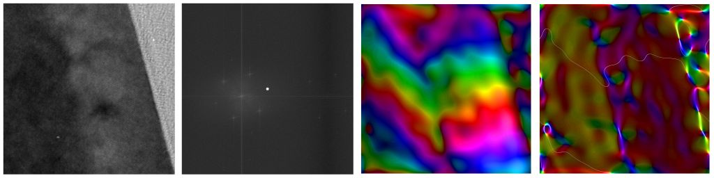
10am29mar2003: Before trying to answer all of these questions,
let's first see if we can move the Fourier aperture and hence the reference
frequency closer to the (002) periodicity on the Si-only side of the lattice.
The stripe colors on that side suggested a tensional strain (larger
lattice spacing than the reference), so we moved the Fourier aperture
downward (closer to the
vertical zero or infinite period) by one pixel. The significantly
improved result is shown
below. As you can see, in panel-3 stripes on the Si-only side have broadened
to almost uniform color, while those on the Ge-Si are more parallel
to the interface. Likewise in panel-4 the strains relative to reference
(especially on the Si-only side) are lower (hence darker in color).
Note: Moving down yet another pixel goes too far, reversing the stripe
sequence on the Si-only side from that in the image set above.

In the above image, we've also taken the liberty of cycling through three different Fourier aperture sizes. As you can see, increasing the bandpass around the frequency of interest increases the the spatial resolution of the image, as well as the amount of possibly unrelated noise.
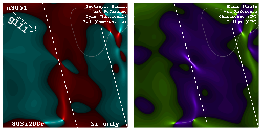
From an (002) "small bandpass" strain analysis of a 36,864 pixel region on the Si-Ge side of this 1024x1024 crop of negative 3051, one finds a strain of magnitude 0.0103+/-.000007 with a net direction 9.8 degrees counter clockwise from the right. This is roughly the direction of the g-vector and surface normal, and thus represents a lattice parameter larger than the reference. The change in phase is 0.0103 [radians per pixel], or 0.0103/2Pi [cycles per pixel]. 2Pi [radians] of course corresponds to a full period phase shift, for Si (002) of about 5.43/2=2.715 [Angstroms per cycle]. Also a 2400 [dpi] (or 2400/2.54 [dots per cm] or 100*2400/2.54 [dots per meter]) scan of a 240,000x image has 1/(240000*240,000/2.54) = 0.44 [Angstroms per pixel]. The change in lattice parameter associated with this is therefore (5.43/2)(.0103/2Pi)=0.00445 [Angstroms per pixel], each of which is 0.44 Angstroms wide. Dimensionless strain is therefore .00445/.44=0.0101+/-.000007. If the silicon has lattice parameter 5.43, the effective lattice parameter of the Si-Ge in that direction must then be 1.0101*5.43=5.485 Angstroms. For 20%Ge-Si we expect a bulk lattice parameter change to .2*5.66+.8*5.43=5.476 Angstroms. This suggests a lattice parameter increase on the Si-Ge side, along (002), of 0.055 Angstroms, about 19% larger than the 0.046 Angstrom increase expected from bulk values. This might be in part due to the strained nature of the overlying silicon, whose lattice we might expect to show compression along (002) even relative to the bulk value for silicon, to compensate for the expansion it is feeling in the interface. When we take into account the residual strain calculated in a patch on the Si-only side, to which we really want to reference our calculation, the conclusion remains essentially the same.
Note: In the process of this analysis, a coordinate-switching error in the calculations on negative 3049, at the top of this page, was discovered. This will have an effect on which areas we thought we were looking at, as well as on interpretation of numeric angles that those calculations gave out. Another bit of good news is that we've now examined relative strain differences between regions of the specimen examined with different reference periodicities (Fourier aperture centering), and find them to be insensitive to this as long as the Fourier aperture is not chopping off the Fourier peak's shape transform. Corrected analysis of the (002) calculation, in the image cut of negative 3049 discussed above, reports an (002) spacing increase (going from Si-only to Si-Ge) of 0.026 Angstroms, about 60% of the 0.046 Angstrom increase expected from bulk values. This might reflect the extreme thinness of the specimen region in negative 3049, in comparison that in negative 3051. Only further analysis of data will tell.
We now turn to the detailed strain variations across the image field. Below find a set of eight 128-line net-amplitude profiles across the panel-4 strain image above. Check out: (a) the drop in strain amplitude as one moves from 80Si-20Ge to Si-only across the tilted interface (which runs from mid-left at top to mid-right at bottom), (b) the bump in strain which marks the interface, and (c) the second bump in strain about 200[pixels]*.44[A/pixel]=88[Angstroms] to the right of the interface bump, when the darker "crinkle" regions are crossed by the profile. Understanding the directions and precise locations of these features could tell us what's happening at the interface, and with the crinkles as well!


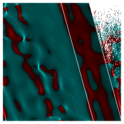
10am1apr2003: Perhaps the most efficient way to see what the data tells us is to break the strain image into istropic and shear components, with respect to the direction of the operating reflection. An example of this is also provided on our model strain page. For the small bandpass analysis of negative 3051 above, we get...
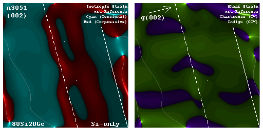
The expanded lattice on the Si-Ge side of the interface (approximately marked with a dashed white line) is now quite apparent in the isotropic strain map, as is the large (002) compressive strain where the transition from Si-Ge to Si-only occurs. This is what is predicted for the Si-only (002) spacing, to compensate for the expansion of the orthogonal (220) spacings needed to maintain coherence at the interface. The isotropic strain then works its way through varying weak (dim) values, out to a weak but comprehensive expansion relative to the reference periodicity at large distances from the interface on the Si-only side. This suggests to me that some strain relief is occurring, just not right at the interface, and not due to dislocations.
The shear strains (right panel) add something else to the story. The white dots mark the center of possible "dark crinkles" in the original brightfield image's intensity. Recall that our strain map tosses all information on periodicity brightness out the window, concentrating only on the lateral position of the fringes (i.e. their Fourier phase). Nonetheless, we may be seeing in the shear map a periodic variation along the interface in lattice shear that maps with the brightness periodicity associated with crinkles. Let's see if this pattern holds up in other places along the interface.
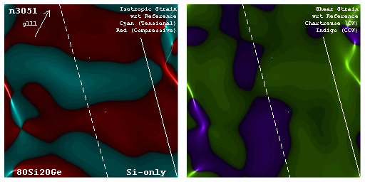
Below find low bandwidth darkfield analysis of negative 3051 using the (111) g-Vector pointed in roughly the 4 o'clock direction.
Note below, as found also in the (002)-reflection isotropic strain map, the compressional zone running along the Si-Ge/Si interface.
Next find a set of low bandwidth strain maps from that first cup of negative 3051, made using the (111) reflection near 1 o'clock. I was surprised to see not isotropic strain, but shear strains tracking the interface in this series. Does this have something to do with interstitial condensations having to choose between the (111) and (111) planes to lie on?
Finally here are low bandwidth strain maps using the weak (220) reflection, lying in the plane of the interface. Do these suggest that "crinkles" are alternating zones of (220) tension and compression? It's too early to tell.

Similarly-oriented coherent-model patterns are now shown at the bottom of our model page, except that the reference periodicity is on the large unit-cell side. Within the context of the model used there, they suggest that (220) strain maps will be featureless, except for possible lateral bunching effects in the 10-nm zone on the Si side of the interface e.g. associated with the crinkles.
A version of that calculation analogous to our (002) case, similarly referenced to the small-cell side of the interface, is shown here. Although for qualitative comparison only, note the strong tension on the large-cell (lower right) side of the interface. Note also the large compression immediately on the upper right side of the interface, where the small-cell spacing in this direction is most actively compensating for the lateral tension it is under. As far as the shear map is concerned, we are currently thinking that the weaker absolute shear is very sensitive to reference location, and in that sense spurious. Meaningful relative shears, of course, could still show through.

9am7apr2003: Over the weekend I ran a very small bandpass (002) strain calculation on a 2kx2k crop from negative 3051. As you can see from the panel set below, the compression band on the Si-side of the interface persists, as does some possible connection between crinkles and alternating shears moving down toward the interface. Likely a larger bandpass calculation on this same reflection is next. After that, a 4kx4k calculation?

9am8apr2003: Here's a version of the same isotropic strain map (computer memory ran out on the shear strain calculation) with bandwidth increased by Sqrt[2] (corresponding to 128 pixel or 6 nm broadening in direct space) so that it is equal to the bandwidth in the 1k calculations (e.g. on 1 Apr) shown above.