Visibility map tips
This is a new window -- resize it for simultaneous viewing of your Live3D model.
Lattice fringes are visible over a wider range of angles if crystals are thinner in the direction of the beam. Microscopes thus see particular lattice spacings only if they're both able to resolve those spacings, and the viewing direction is within the thickness-dependent band of visibility for that spacing. Fringe-visibility maps describe the fringes a microscope will see on crystals of given thickness, plus the orientation relationship between those fringes. Such maps thus characterize the fringe patterns seen in a collection of randomly-oriented nanoparticles*, and can guide tilt experiments to fully determine the lattice of any specific particle**. Their layout is like that of Kikuchi maps*** except that larger lattice spacings give rise to wider, rather than narrower, bands. Blank spaces (external to fringe bands) on the "visibility sphere" represent orientations at which no lattice fringes are seen. You can read more about fringe visibility maps here.
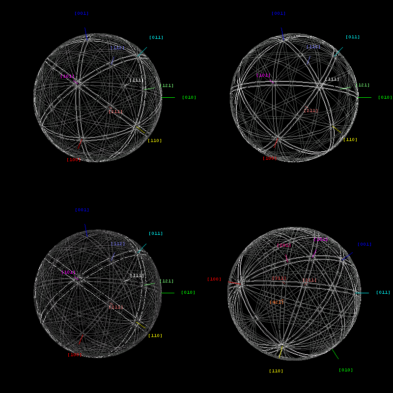
Microscope orientations are referenced to a given lattice by zone (or direct lattice uvw) indices, while crystallographic planes are described by Miller (or reciprocal lattice hkl) indices. Zones are perpendicular to lattice plane-normals when uh+vk+wl=0, and therefore label intersections between planes. When crystals are cubic, zones are also parallel to plane-normals with similar indices. Zone indices for the current viewing direction can be listed by clicking the [Zone Indices] button. Likewise, angular rotation distances between the present viewing direction, and the last indexed zone, can be determined under any viewing conditions by clicking the [Angle to LastZone] button.
Presently we're using 300kV electrons for all vMap plots, and we've set physical dimensions for the sphere diameter to the specimen thickness t being used in the calculation. On some maps we also subdivide visibility bands into four strips, so that fringe symmetry at zone crossings is apparent. However, the geometry of "viewing through a tube" of length t dictates that the physical fringe spacing will be radius times twice the visibility half angle, or the band thickness itself. Note: If you wish to measure band widths (lattice spacings) in these visibility plots, it's best to first increase camera focal length by repeatedly dragging the mouse up with the [Control] key down. In this way, perspective effects in front of the rotation center won't result in overestimates of the spacing.
The mouse allows you to re-orient and or spin the specimen, while the [Shift] key plus vertical mouse motion allows zooming in on the model for a much, much, much, MUCH closer look. The [Shift] key plus horizontal mouse motion rotates the image in the viewing plane, and the [Home] key returns you to the original point of view. "Javascript buttons" below the live image let you estimate field-width, goniometer angles, and/or a variety of other parameters. The rotation-center may be moved with respect to a set of cartesian (xyz) axes fixed to the microscope by tapping the [x][X][y][Y][z][Z] keys (hint: rotate between taps). The [Control] key plus vertical mouse motion allows you to change the focal length of your view, in effect altering "the perspective effect". For small models, the "s" key generates stereopairs, whose angular separation can be adjusted with the [Control] key plus horizontal mouse motion.Footnotes:
* For example, the probability of encountering a given cross-fringe pattern is proportional to the area of band intersections at the corresponding zones (cf. arXiv:cond-mat/0212281).
** For example, lattice parameters can be measured on individual nanoparticles from images taken at two carefully selected large-angle tilts (cf. Ultramicroscopy 94, 2003, 245-262), and protocols for approaching complete unknowns using aberration-corrected microscopes were described e.g. at T.E.A.M. 2003.
*** One or more test Kikuchi map models are now on the menu. Being reciprocal space structures, (like the Ewald) sphere diameter is 2/wavelength and band widths are 1/d. Feel free to send in requests for specfic structures until we get webMathematica versions on-line so you can "roll your own".
The frames host for this page is (http://www.umsl.edu/~fraundor/nanowrld/live3Dmodels/vpmapframe.htm). As an experimental page, there are no guarantees of correctness, and suggestions toward improvement are invited. Although there are many contributors, the person responsible for errors is P. Fraundorf. This site is hosted by the Department of Physics and Astronomy (and Center for Molecular Electronics) at UM-StLouis.