
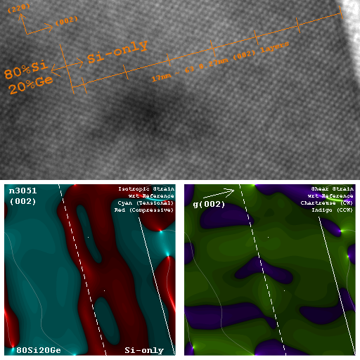
This page, on a note concerning a seldom-discussed feature of ion-milled silicon surfaces, was corollary to decades of work by researchers in this lab on a wide range of silicon science problems. A composite figure at the bottom of this page (like the figure on sub-picometer vector-strain mapping at right) may provide some clues, but that too only selects incidentals. Much of our work has been done in collaboration with researchers (some of them graduates from here) working for MEMC/SunEdison-Semiconductor (since 1959 a major supplier of silicon to the integrated-circuit industry), in the process of which we have perhaps the largest collection of device-industry related silicon-science transmission-electron-microscope (TEM) specimens on the planet.
Most recently, we've published notes [1-3] on the connection between the surface-intrusions discussed in this paper, and the larger problem of understanding the role of oxygen-cluster nucleation (and growth) in Czochralski silicon, as a function of thermal history during growth as well as in the device manufacturing/operation process. This is important to the industry because oxygen-related defects play a powerful role in trapping impurities, in strenthening wafers, and in generating silicon self-interstitials, as well as in the semiconducting behavior of the material itself.
[1] Jamie Roberts, P. Fraundorf, Jai Kasthuri and David Osborn (2016) "Exploring Boltzmann-Factor Distributions of Precipitation-Nuclei in the TEM", Microscopy and Microanalysis 22:S3, 942-943 Cambridge hal-01367881 pdf.
[2] P. Fraundorf, Jamie Roberts and David Osborn (2017) "Exploring sub-10[nm] oxygen clusters in Czochralski silicon" (59th MRS Electronic Materials Conference, U. Notre Dame, South Bend IN) pdf.
[3] Jamie Roberts, David Osborn and P. Fraundorf (2017) "Finding unstrained 10-nm lattice defects in Si given 10^11/cc", Microscopy and Microanalysis 23:S3 (in press) pdf.
One might say that this paper offers the first systematic consideration of tiny defects that form spontaneously at room temperature on silicon surfaces prepared by a variety of methods*, but which have so far been possible to ignore because of their small size and weak strain fields. Experiments on the internal gettering (trapping) of impurities in gigascale integrated circuit silicon (computer chips) during device manufacture created the need for this study, because the size of gettering defects in the silicon interior has now moved down into the 10 nm (50 atoms on a side) range. These surface defects might, if present, show up in diffuse scattering of light from wafers, and we expect that they will become more significant (as possible allies and adversaries) when devices on silicon become smaller still. The apparent limit on number density observed for these, and similar, defects at silicon surfaces also suggests that a surface hardening effect at air-exposed silicon surfaces (perhaps like the formation of a film on cooling but unstirred soup) may be involved./pf 2002oct02
* These defects were found to be ubiquitous, but oft only weakly visible, on air-exposed transmission electron microscope specimens prepared, by acid-etching as well as ion-milling, from integrated circuit silicon of the many crystallographic orientations, dopant types, ingot positions, and thermal histories enountered in over three decades of work with silicon grown by numerous major wafer manufacturers.
Sound Bytes: spontaneously-forming raisin/raspberry defects |
wafer complexions | silicon surface hardening?
Lin02.10nm PDF 2002 (c) The ElectroChemical Society (posted with permission)
BiBTeX reference:
@article{Lin02.10nm,
author = "Shu-han Lin and Iris Mack and Noom Pongkrapan and P. Fraundorf",
title = "Ten nanometer surface intrusions in room-temperature silicon",
journal = "Electrochemical and Solid-State Letters",
volume = "5",
number = "9",
pages = "G83-G85",
year = "2002",
eprint = "arXiv:cond-mat/0110393"}


An early HREM image of a tiny defect down [100]...
Two 10 nm defects superposed on crossed 0.192nm (220) frings in a thinned [001] silicon specimen...
and a image set with thickness fringes for analyzing surface and volume related correlations...
Sequential (green, then red) HREM images of a three-defect cluster seen in the above series...
and a closer look at the two defects together in the later image, wherein the crossed 0.192 nm silicion (220) lattice spacings can be seen superposed...
TEM, SPM Studies on Ten Nanometer Surface Intrusions in Room-Temperature Silicon
Shuhan Lin, P. Fraundorf, and Noom Pongkrapan
Physics and Astronomy and Center for Molecular Electronics
University of Missouri-StL, St. Louis, Missouri 63121
We describe here defects between 5 and 15 nm in size, with number densities near 10^10 cm^{-2}, which form spontaneously after exposure to air beneath silicon surfaces newly-formed by ion-milling or an acid-etch with or without a post-etch dip in HF. The process of their formation at room temperature can be slowed to laboratory time scales, if air exposure is shorter than 8 minutes, allowing subsequent in situ observation of their nucleation and growth via TEM and HREM. Needless to say, defects of this sort could be either allies or adversaries of device manufacture, as device sizes move into the nanometer range.
Electron diffraction contrast and HREM imaging experiments indicate that the most common of these defects are weakly strained amorphous intrusions into (100), (110), or (111) silicon surfaces, approximately 10 nm in size in all three directions, reminiscent of tenth-micron sized "s-pit" related defects caused by heating iron and nickel contaminated silicon wafers at high temperature [2]. Weakly strained crystalline defects similar in size and number density, which show Moire contrast and diffraction effects similar (if not precisely the same as) colony copper silicide precipitates which decorate stacking faults in bulk silicon [3], have also been found on rare specimens [4].
The weak strain fields (compared to defects in the bulk), and common number density and size of all of these defects on new silicon surfaces, relatively independent of: (i) the method of surface formation, (ii) the crystallographic orientation of the Si surface, (iii) the prior dopant and process history of the silicon examined, and (iv) even the nucleating species and type of defect, suggests that a process of silicon surface hardening, e.g. associated with the buildup of compressional strain at the Si surface, may be limiting further defect formation and size.
Limiting the air exposure of both ion milled and HF-dipped acid etched surfaces to only a few minutes, in our lab, slowed down the formation of the amorphous intrusions sufficiently that the process of both nucleation and growth appears to be observable in the transmission electron microscope [1,5], where the exponential fit characteristic (e-folding) time for nucleation in both cases was in the 10-30 hour range. Time elapsed between nucleation and growth to full size, however, was much less than one hour.
Work is presently underway to (i) observe the real-time nucleation and growth process via HREM with finer time resolution, and (ii) to characterize any changes in surface topography associated with these defects via either SPM or shadow replication.
Here find a table of other incidental topics which have come up in our long history of work on silicon for the integrated-circuit industry.

